As semiconductor manufacturers push the boundaries of chip packaging technology, industry experts are examining the physical and economic constraints that could slow further progress. Advanced packaging techniques like chiplets and 3D stacking have enabled continued performance gains, but thermal management, yield rates, and manufacturing costs are becoming critical bottlenecks. The industry faces a pivotal moment where incremental improvements may no longer suffice, forcing a reckoning with fundamental engineering limits.
OpenAI is hosting a livestream event. Details about the specific announcements, product launches, or demonstrations will be revealed during the broadcast.
The last time OpenAI did an unannounced livestream, they dropped GPT-4 Turbo and changed pricing overnight
OpinionsRead
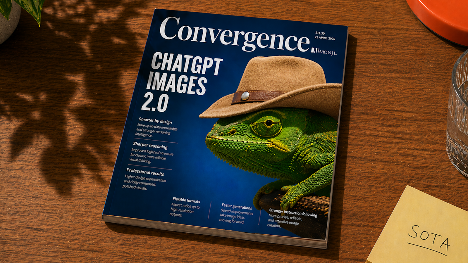
ChatGPT Images 2.0
OpenAI is launching ChatGPT Images 2.0 with major upgrades to image generation capabilities. Watch the livestream announcement at https://openai.com/live/
OpenAI is positioning this as a direct competitor to established image generation tools, suggesting they're confident enough to challenge the current market leaders
OpinionsRead
The "just wait 6 months" argument from 2025 survived exactly one iteration
Throughout 2025 the standard response to any complaint about an LLM was some version of "just wait 3-6 months, the next generation will handle this effortlessly." The argument was everywhere. Every limitation was temporary, every missing capability was a few iterations away, every autonomous agent demo was a preview of imminent reality.
It's April 2026 now and worth checking how that held up.
On r/ClaudeAI this week there's a long thread about Opus 4.7 where multiple users argue it's a regress
OpinionsRead
Mistral Medium 3.5 on AMD Strix Halo: Painfully Slow (Plan for Overnight Runs)
Someone actually tested Mistral Medium 3.5 on AMD's new Strix Halo chip, and the results are... not great. For a 48k-token prompt with 4k thinking tokens, it took about 2 hours just to get an answer about code architecture. Yeah, you read that right—two hours. The takeaway: if you want to run this locally on Strix Halo, queue it up before bed. The technical setup involved heavy optimization (Q5_K_XL quantization, GPU acceleration with -ngl 999, cache reuse), but even with all that tuning, it's still a crawl. Not exactly the "instant local AI" dream, but hey, at least it works.